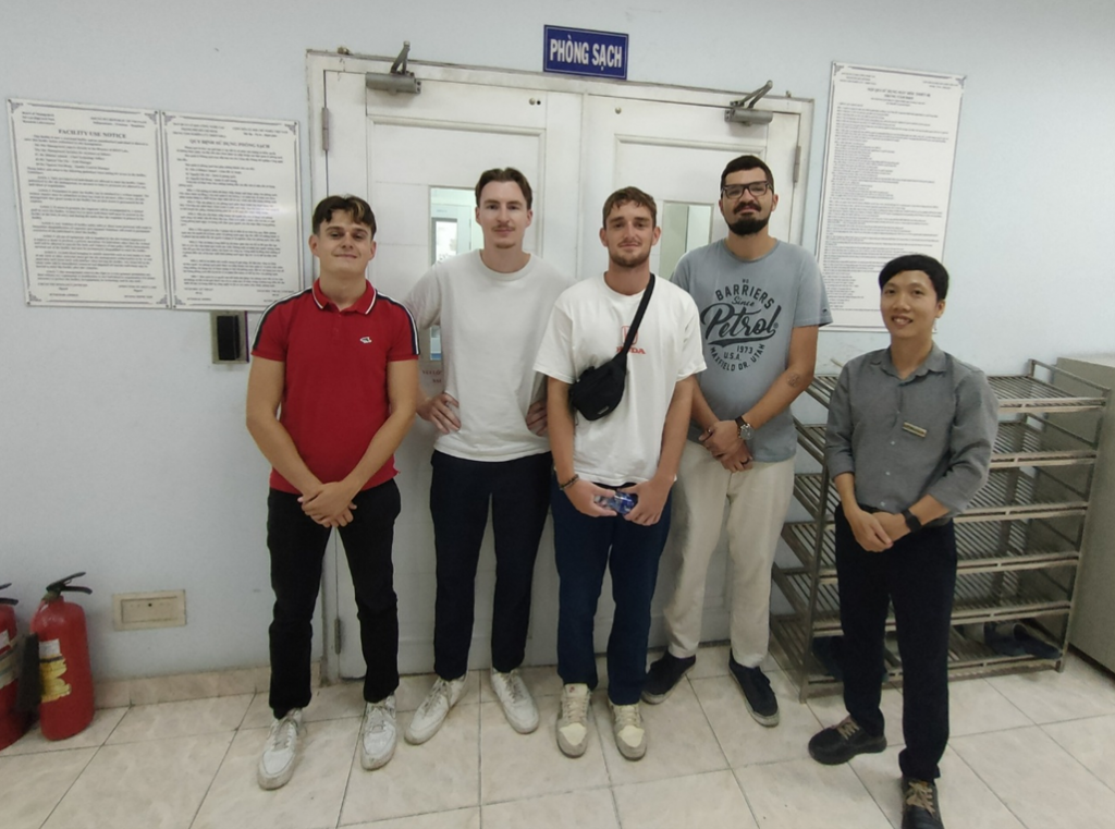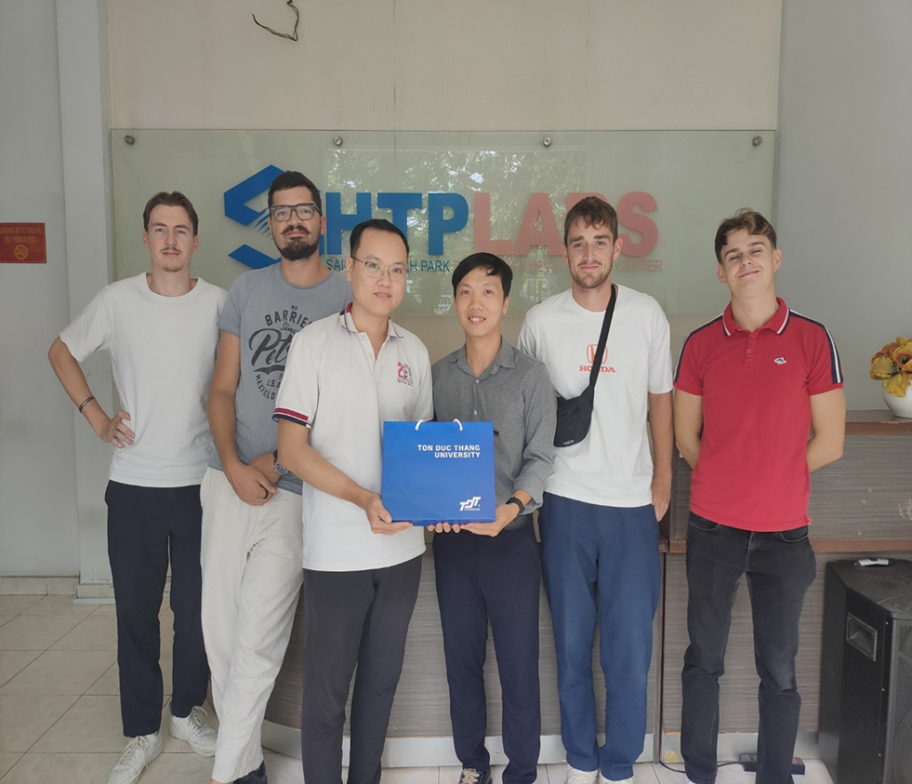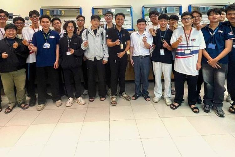
Students of the Faculty of Electrical and Electronics Engineering visit the Research and Development Center – Sai Gon High-tech Park
In order to help students have a comprehensive view of knowledge related to the fields of electricity and electronics in practice at enterprises; on July 25, 2025, the Faculty of Electrical and Electronics Engineering (FEEE) of Ton Duc Thang University (TDTU) coordinated with the Research Laboratories of Saigon Hi-Tech Park in Ho Chi Minh City (SHTPLabs) to organize a visit for students to a modern laboratory on nano and semiconductor technology. The visit was attended by international students who are doing student exchange at the FEEE.
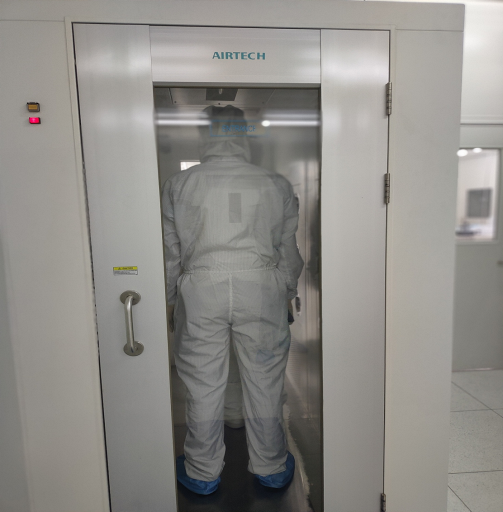
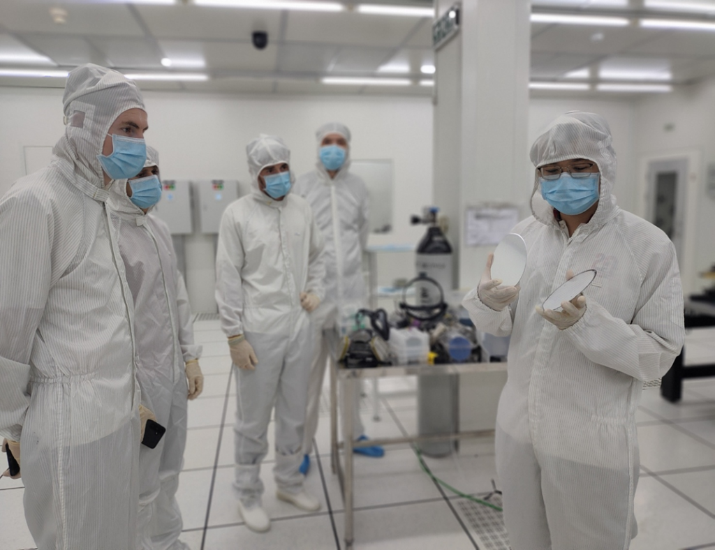
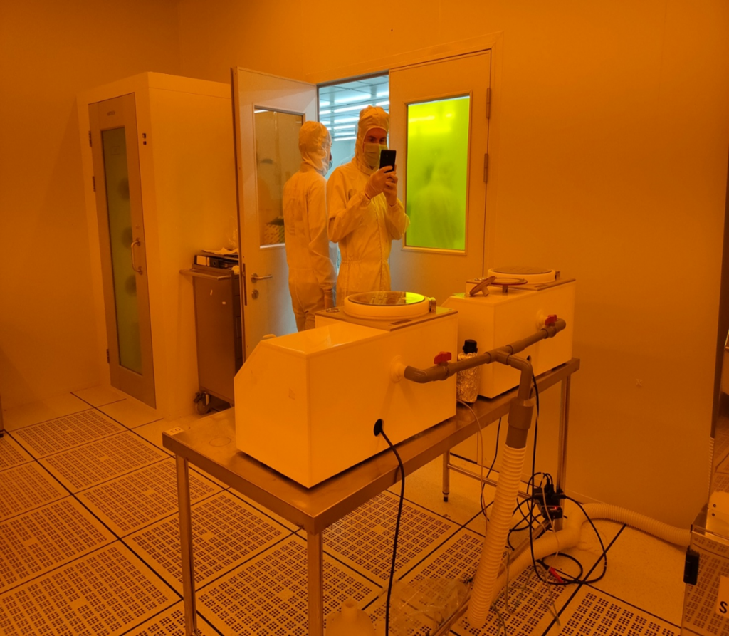
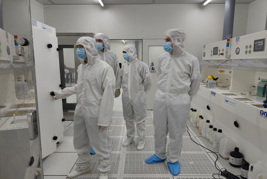
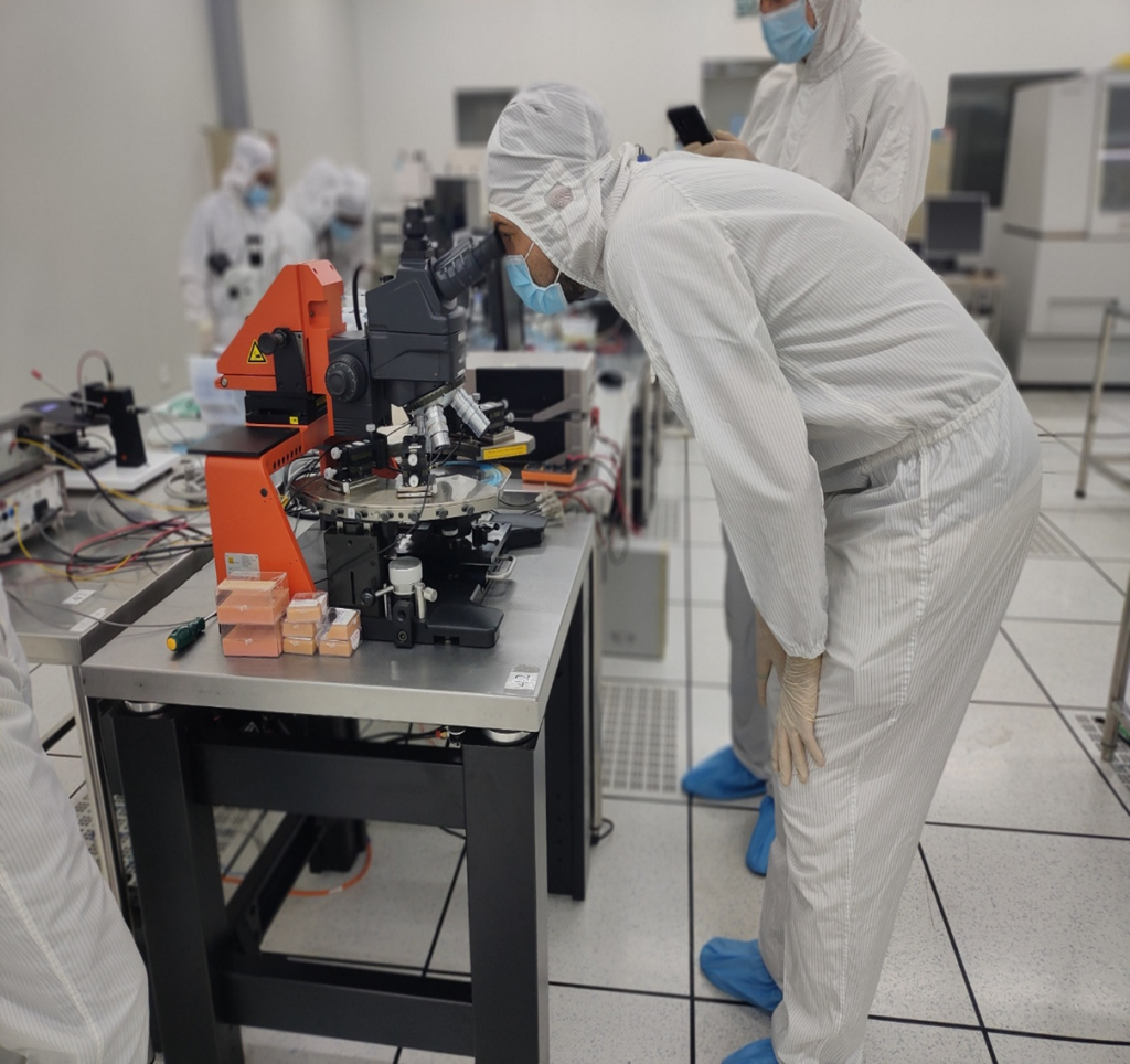
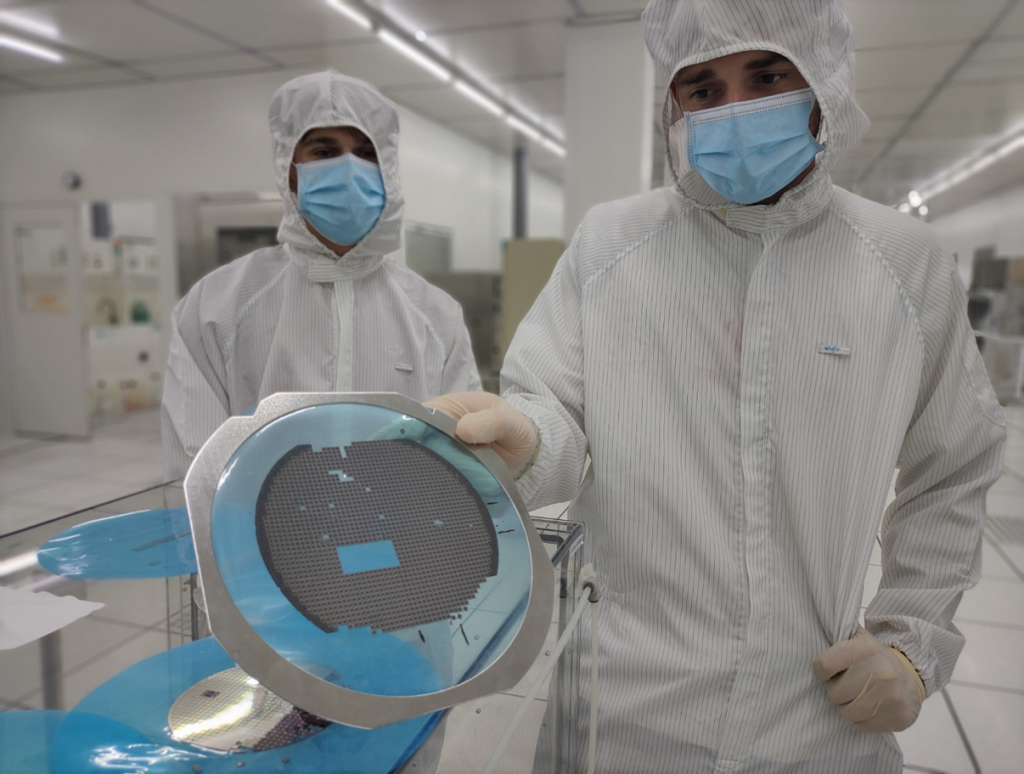
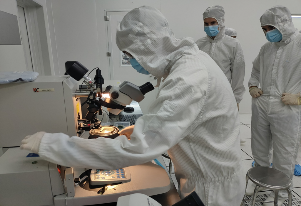
SHTPLabs introduced to the students of the FEEE about the cleanroom and the semiconductor products manufactured here, typically pressure sensors, flow sensors, force strain sensors, and biological sensors. The students were able to fully visit the four semiconductor microchip manufacturing areas: wafer processing, photolithography, chemical etching, testing, and packaging. The manufacturing areas are located in the corresponding cleanroom levels: class 10000 for wafer processing, class 1000 for packaging, and class 100 for photolithography and chemical processing. Students were able to observe the products at each processing stage under a microscope, and were explained about the microchip manufacturing process. The center also introduces internship programs for students in the laboratories at the center: Nano Technology Lab, Semiconductor Lab, Precision Mechanics and Automation Lab, Biotechnology Lab and Information Technology Lab.
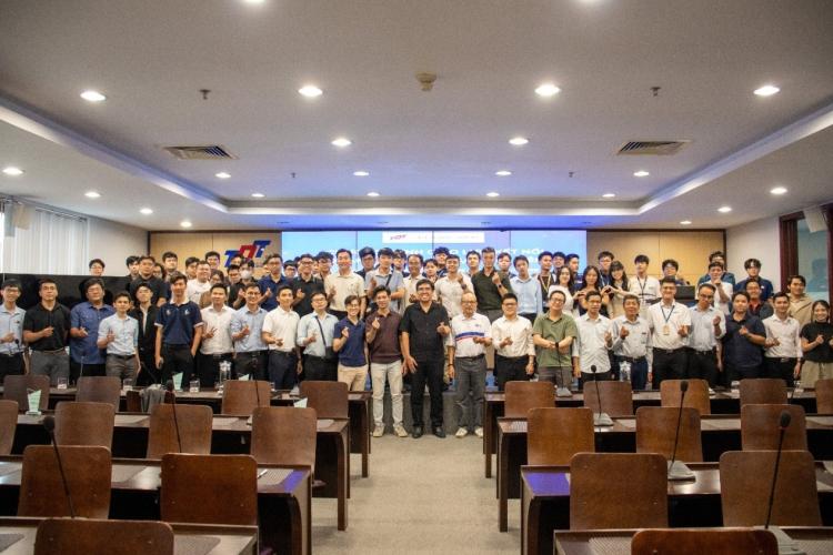
At the end of the visit, representatives of the FEEE, TDTU presented gifts and took souvenir photos with representatives of the center. The trip expanded practical knowledge about clean room technology for students of the FEEE in the context of semiconductor design becoming a hot trend today. The network of partners and business relations of the FEEE always accompanies and provides maximum support to students of the FEEE in developing their careers.
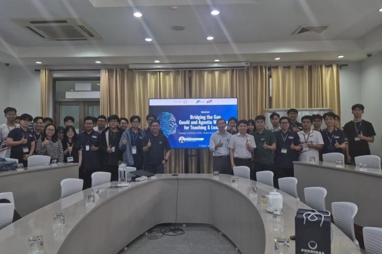
Some photos during the visit: